 |
Nanoscopy Lab
 |
The interaction of materials with intense electromagnetic radiation modifies the topography and physico-chemical properties of their surfaces [1]. The top layers are ejected from a surface in the extreme case called ablation. Ablation efficiency can be evaluated from the global properties of ablation craters (diameter, depth, shape) dependent on the properties of the incident radiation. A detailed look at the damaged surfaces shows the redistribution and phase transformation of the radiation-affected material. These observations, supported by the results of in situ diagnostics, give insight in to the mechanisms of the interaction between matter and radiation, in our case XUV and/or X-ray, i.e. short-wavelength radiation.
Laser- induced periodic surface structures (LIPSS) [2,3] are interesting phenomena following laser ablation. According to the nature of their origin LIPSS of two kinds can be distinguished. Most of the observed LIPSS-I have a spatial period and orientation strongly dependent on the laser properties (wavelength, polarization, coherence, angle of incidence). They are created due to the interference of the incident laser beam with a field scattered along a surface. Structures of the second kind (LIPSS-II) have spatial periods that are significantly greater than the laser wavelength and depend more on laser intensity than wavelength, when a short-wavelength laser is used for surface irradiation.
[1] D. Bauerle: Laser Processing and Chemistry, 2nd Ed., Springer-Verlag, Berlin, 1996.
[2] A. E. Siegman and P. M. Fauchet: IEEE J. Quantum Electron. QE–22, 1384–1403 (1986).
[3] J. E. Sipe, J. F. Young, J. S. Preston
and H. M. van Driel: Phys. Rev. B
27, 1141–1154 (1983).
|
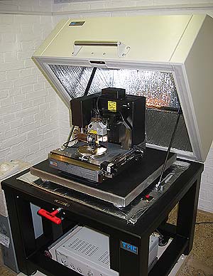
The Nanoscopy Lab was established at the Institute of Physics in 2004 as a joint laboratory of the Department of Laser Plasmas and the Department of Thin Films. The laboratory is equipped with a Dimension 3100 Scanning Probe Microscope (Veeco) controlled by a NanoScope IV Control Station (Veeco). This layout represents a unique tool for analysis of irradiated surfaces due to the fast and easy application of atomic force microscopy (AFM) and scanning tunneling microscopy (STM) techniques.
|
 |
|
|
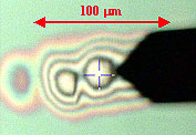
Optical micrograph |
The following characteristics, among others, deserve to be highlighted:
- large samples (up to 200 mm diameter and 12 mm thick) can be investigated
- optical microscopy allows accurate specification of cantilever initial position (see the picture above)
- topography of large areas can be explored by AFM in tapping mode, e.g. 60 micron × 60 micron scan can be measured with a tip velocity 10 microns/s
- detailed images with a resolution of ~ 10 nm can be obtained in various not only topographical modes, e.g. image of electrical or magnetic properties
- SPM is operated in the air but isolated from vibrational and electrical noise from surroundings
A Nomarski BX51 microscope equipped with a digital camera C5060 (both from Olympus) is available in the Nanoscopy Laboratory.
